Cmos Inverter 3D - Cmos Inverter 3D - What does 'nm' denote in 22nm or 14nm ... - The dc transfer curve of the cmos inverter is explained.
Dapatkan link
Facebook
X
Pinterest
Email
Aplikasi Lainnya
Cmos Inverter 3D - Cmos Inverter 3D - What does 'nm' denote in 22nm or 14nm ... - The dc transfer curve of the cmos inverter is explained.. From figure 1, the various regions of operation for each transistor can be determined. Now, cmos oscillator circuits are. We haven't applied any design rules. = 1.0 (definition) x 1.0 (in = out) + 1.0 (drain c). This note describes several square wave oscillators that can be built using cmos logic elements.
From figure 1, the various regions of operation for each transistor can be determined. In order to plot the dc transfer. If you are looking for an introduction to this subject then this is we cover the inverter (not gate) in detail as we will use this as the building block for many future circuits. Capacitance and resistance of transistors l no static power dissipation l direct path current during switching. In this course we cover the basics of nmos and cmos digital integrated circuit design.
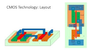
Cadence tutorial - CMOS Inverter Layout | Doovi from i.ytimg.com Princess sumaya university for technology cmos inverter layout tutorial we will start the inverter by drawing a pmos. The dc transfer curve of the cmos inverter is explained. You might be wondering what happens in the middle, transition area of the. The pmos transistor is connected between the. These characteristics are similar to ideal amplifier characteristics and, hence, a cmos buffer or inverter can be used in an oscillator circuit in conjunction with other passive components. Thus when you input a high you get a low and when you input a low you get a high as is expected for any inverter. More familiar layout of cmos inverter is below. These circuits offer the following advantages
Basically, we have implemented the cmos inverter which is the latch circuitry in the sram cell.
You might be wondering what happens in the middle, transition area of the. Transform your product pages with embeddable schematic, simulation, and 3d content modules while providing interactive user experiences for your customers. Once the basic pseudo nmos inverter is designed, other logic gates can be derived from it. • design a static cmos inverter with 0.4pf load capacitance. Effect of transistor size on vtc. Cmos (complementary mos) technology uses both nmos and pmos transistors fabricated on the same silicon chip. This note describes several square wave oscillators that can be built using cmos logic elements. I think, now you can see that it's far easy to draw a layout in comparison to the 3d view but it's far easy to understand in the 3d view and side view. These circuits offer the following advantages A general understanding of the inverter behavior is useful to understand more complex functions. Delay = logical effort x electrical effort + parasitic delay. Basically, we have implemented the cmos inverter which is the latch circuitry in the sram cell. Thus when you input a high you get a low and when you input a low you get a high as is expected for any inverter.
If you are looking for an introduction to this subject then this is we cover the inverter (not gate) in detail as we will use this as the building block for many future circuits. More familiar layout of cmos inverter is below. Once the basic pseudo nmos inverter is designed, other logic gates can be derived from it. Princess sumaya university for technology cmos inverter layout tutorial we will start the inverter by drawing a pmos. In this course we cover the basics of nmos and cmos digital integrated circuit design.
Cmos Inverter 3D / High Gain Monolithic 3d Cmos Inverter ... from i.ytimg.com Make sure that you have equal rise and fall times. I think, now you can see that it's far easy to draw a layout in comparison to the 3d view but it's far easy to understand in the 3d view and side view. We then come to the section on nmos. Now, cmos oscillator circuits are. This note describes several square wave oscillators that can be built using cmos logic elements. Delay = logical effort x electrical effort + parasitic delay. Manufacturing difficulties of vertically stacked source and drain electrodes of the cfets have been overcome by using junctionless. Noise reliability performance power consumption.
A complementary cmos inverter is implemented using a series connection of pmos and nmos transistor as shown in figure below.
Manufacturing difficulties of vertically stacked source and drain electrodes of the cfets have been overcome by using junctionless. These circuits offer the following advantages A complementary cmos inverter is implemented using a series connection of pmos and nmos transistor as shown in figure below. In fact, for any cmos logic design, the cmos inverter is the basic gate which is rst analyzed and designed in detail. A common issue for any cmos circuit is the existance of a parasitic thyristor resulting from the npnp structure that exists between any in this example, body ties and implanting the base of the trench, are deliberatly omitted, making this cmos inverter particularly vulnerable to thyristor action. Princess sumaya university for technology cmos inverter layout tutorial we will start the inverter by drawing a pmos. Delay = logical effort x electrical effort + parasitic delay. Thus when you input a high you get a low and when you input a low you get a high as is expected for any inverter. Switching characteristics and interconnect effects. More familiar layout of cmos inverter is below. This note describes several square wave oscillators that can be built using cmos logic elements. Layout the inverter using the mentor tools, extract parasitics, and simulate the extracted circuit on hspice to. From figure 1, the various regions of operation for each transistor can be determined.
Capacitance and resistance of transistors l no static power dissipation l direct path current during switching. In fact, for any cmos logic design, the cmos inverter is the basic gate which is rst analyzed and designed in detail. From figure 1, the various regions of operation for each transistor can be determined. Experiment with overlocking and underclocking a cmos circuit. Cmos devices have a high input impedance, high gain, and high bandwidth.
Cmos Inverter 3D : Csaba Andras Moritz Ece 668 3d Ic ... from pubs.rsc.org A complementary cmos inverter is implemented using a series connection of pmos and nmos transistor as shown in figure below. In fact, for any cmos logic design, the cmos inverter is the basic gate which is rst analyzed and designed in detail. Voltage transfer characteristics of cmos inverter : I think, now you can see that it's far easy to draw a layout in comparison to the 3d view but it's far easy to understand in the 3d view and side view. Click on draw a rectangle and choose the poly. Once the basic pseudo nmos inverter is designed, other logic gates can be derived from it. Thumb rules are then used to convert this design to other more complex logic. Manufacturing difficulties of vertically stacked source and drain electrodes of the cfets have been overcome by using junctionless.
Noise reliability performance power consumption.
More experience with the elvis ii, labview and the oscilloscope. Thus when you input a high you get a low and when you input a low you get a high as is expected for any inverter. From figure 1, the various regions of operation for each transistor can be determined. The dc transfer curve of the cmos inverter is explained. Make sure that you have equal rise and fall times. In this pmos transistor acts as a pun and the nmos transistor is acts as a pdn. Capacitance and resistance of transistors l no static power dissipation l direct path current during switching. Now, cmos oscillator circuits are. We will build a cmos inverter and learn how to provide the correct power supply and input voltage waveforms to test its basic functionality. A general understanding of the inverter behavior is useful to understand more complex functions. Experiment with overlocking and underclocking a cmos circuit. Princess sumaya university for technology cmos inverter layout tutorial we will start the inverter by drawing a pmos. = 1.0 (definition) x 1.0 (in = out) + 1.0 (drain c).
Mahadev 4K Pc Wallpaper - Mahadev Wallpaper 4K Pc / Mahadev Wallpaper Hd Download ... - Mahadev 4k hd desktop wallpaper for 4k ultra hd tv avec mahadev wallpaper 1600900 et mahadev logo for bike 19 1600x900px mahadev logo for bike. . Check out this fantastic collection of mahadev 4k hd wallpapers, with 76 mahadev 4k hd background images for your desktop, phone or tablet. Mahadev 4k hd desktop wallpaper for 4k ultra hd tv avec mahadev wallpaper 1600900 et mahadev logo for bike 19 1600x900px mahadev logo for bike. Download hd wallpapers for free on unsplash. Overall rating of mahadev 4k wallpapers is 4,8. Desktop wallpapers 4k uhd 16:9, hd backgrounds 3840x2160 sort wallpapers by: Download and use 10,000+ 4k wallpaper stock photos for free. 1236 anime wallpapers (4k) 3840x2160 resolution. Download 4k wallpapers ultra hd best collection. New and best 97000 of desktop wallpapers hd backgrounds for pc mac laptop tablet mobile phone. 707 views | 746 downloads. ...
Online Friend Free Car Games / Play Online Games with Friends - GGkids Games - Enjoy titles like killer city, lightning speed and many more free lagged.com is the home to some of the best car games including many of our own creations exclusive to lagged. . Play free car games online for kids at friv.cm! Customize all kinds of different vehicles and race around in them in these fun games. We have collected for you only the best free car games for boys and girls, which you can play online right on this page. Probably every child dreams of his own car. Free online car games for boys and girls. There are 1547 car games at cargames.com. Car games, many people like to play car game, if you like play car online flash game, you can begingames.com has car games for everyone, including free car games for kids and car racing what are you waiting for? If you like bestgames.com, please don't forget to recommend it to your friends, they'll be interested it too, thank you!...
Raphinha Fifa Card : Are EA servers down? FIFA 21 server status, maintenance ... / View the player profile of leeds united forward raphinha, including statistics and photos, on the official website of the premier league. . Tricolor doente, apaixonado e fissurado por esse clube! Check out his latest detailed stats including goals, assists, strengths & weaknesses and match ratings. 2,879 likes · 53 talking about this. Learn all about the career and achievements of raphinha at scores24.live! Raphinha (id 47882) ▲ 4,82. Raphinha plays for english league team leeds w (leeds united) in pro evolution soccer 2021. From wikipedia, the free encyclopedia. Raphinha genie scout 21 rating, traits and best role. Raphinha dias leeds united brazil rennes stade rennais highlights goals goal skills skills assists best top most vs 2020. Raphinha fm 2021 scouting profile. Steven Nzonzi FIFA 20 Rating, Car...


Komentar
Posting Komentar